
How to Assemble a Printed Circuit Board
This SOP describes the end-to-end PCB assembly process at the Roy Electronics facility, from bare board serialization through final testing and delivery. It documents how Valor Manufacturing Solutions, Valor Process Preparation, Valor Material Management, Valor IoT, and the CamStar Electronic Suite integrate across the shop floor to ensure traceability, quality control, and process efficiency.
Video: PCB 101 Academy - Learn how printed circuit boards are assembled by Siemens Software (2020). All credit for the demonstration goes to the creator; watch the original on YouTube. The written guide below was generated from this video by Docsie. Creator? Request a change or removal.
Purpose
This SOP describes the end-to-end PCB assembly process at the Roy Electronics facility, from bare board serialization through final testing and delivery. It documents how Valor Manufacturing Solutions, Valor Process Preparation, Valor Material Management, Valor IoT, and the CamStar Electronic Suite integrate across the shop floor to ensure traceability, quality control, and process efficiency.
Scope
This procedure applies to operators, quality control personnel, and process engineers involved in Industry 4.0 PCB assembly operations, including solder paste application, component placement, inspection, soldering, electrical testing, and final product delivery at the Roy Electronics facility.
Required Equipment and Systems
- Laser marking machine (e.g., NEOMARK easy)
- ERP (Enterprise Resource Planning) system
- Valor Process Preparation software
- Valor Material Management software
- Valor IoT Manufacturing system
- Screen printer with job-specific stencils
- Solder Paste Inspection (SPI) machine (e.g., KY 8030-2)
- Pick and place machines: high-speed, camera-guided, and high-force variants (e.g., SIEMENS SIPLACE, ASM Assembly Systems)
- Visual inspection station
- Reflow oven with multiple temperature/speed chambers
- Automated Optical Inspection (AOI) machine (e.g., Omron VT-RNS)
- Selective soldering oven for through-hole/manual assembly (e.g., ERSA VERSAFLOW 3/45)
- Electrical test equipment: Bed of Nails and Flying Probe testers (e.g., SPEA 3030 Board Tester)
- CamStar Electronic Suite
- X-ray inspection system
- Opcenter Execution Electronics
Safety note: X-ray inspection stations are marked with warning signs. Operators must observe posted X-ray safety precautions when working at this station.
Procedure
Phase 1: Facility overview and shop floor introduction
Step 1 — Arrive at the facility. Roy Electronics is located in Northern Italy in a large, modern industrial complex surrounded by greenery and other industrial buildings. The main building is labeled "ROJ" and features solar panels on the roof.

Step 2 — Enter the Industry 4.0 assembly shop floor. The production floor is highly automated, with minimal human operators visible. The environment is clean, organized, and equipped with modern assembly machines.
Step 3 — Observe automated material handling. Automated guided vehicles (AGVs) or robots transport PCB racks between stations. The system includes pass/fail sorting stations for quality control, and the floor is marked for robot navigation.
Phase 2: PCB serialization and traceability
Step 4 — Mark each PCB with a unique serial number. Feed the bare PCB into the laser marking machine. The machine marks a unique serial number, generated by the ERP system, on each board and reports the number to an output file for collection by the Valor IoT system.
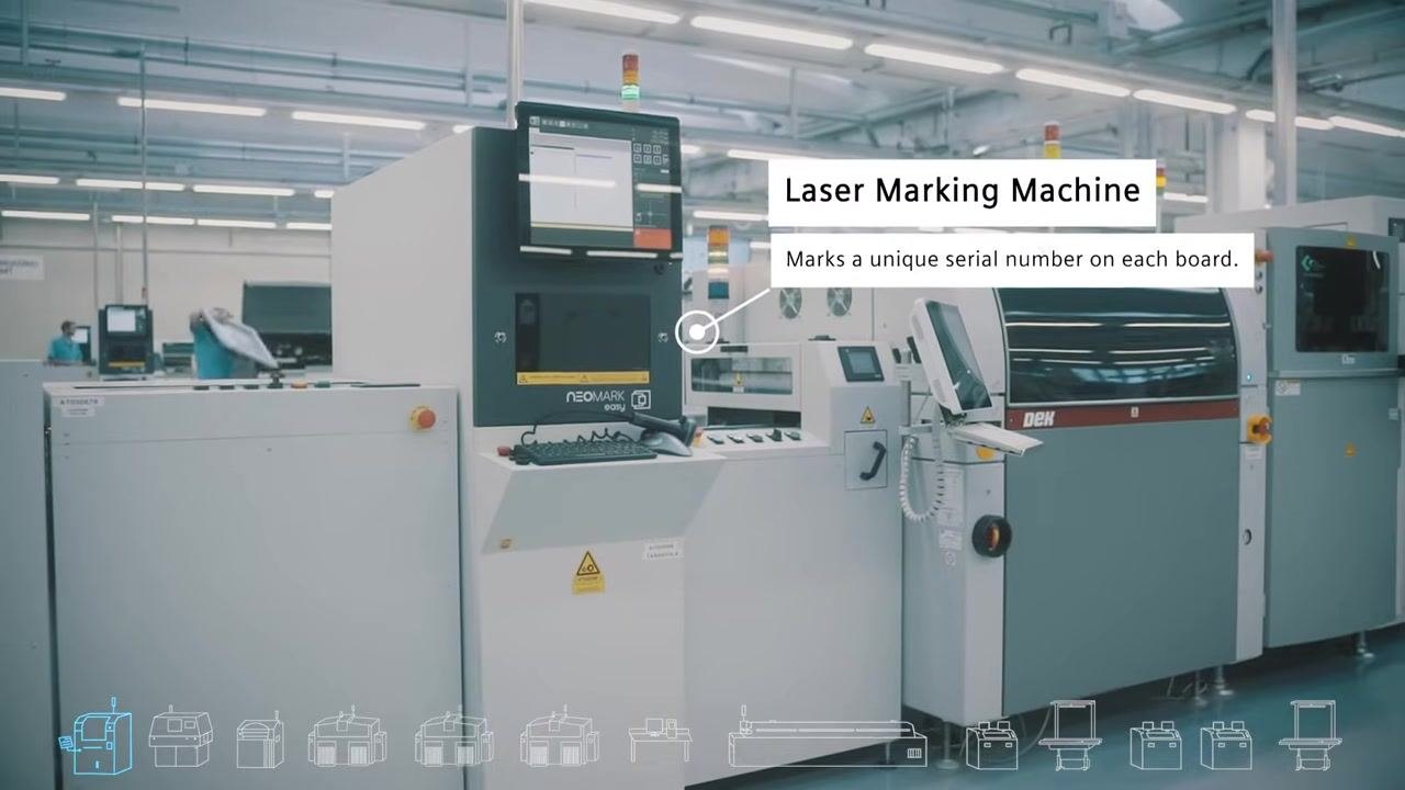
Step 5 — Confirm ERP serial number management. Verify that the ERP system is generating and tracking unique serial numbers for each PCB throughout production. System status may be shown as a progress indicator (e.g., ERP 74%).
Step 6 — Confirm ERP integration with Valor Process Preparation. Ensure the ERP system communicates with Valor Process Preparation so that each job is planned precisely per product and revision. Integration status may display as, for example, ERP 100% and Valor Process Prep 61%.
Phase 3: Solder paste application and stencil verification
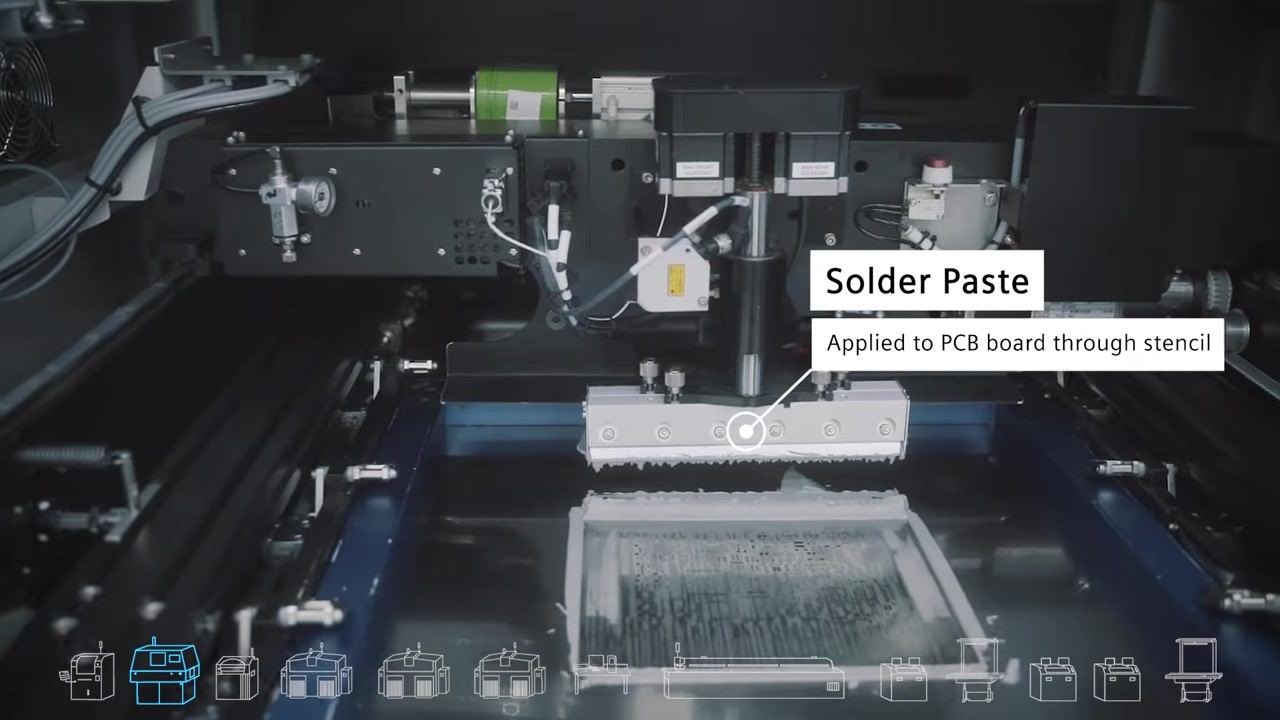
Step 7 — Apply solder paste. Use the screen printer to apply solder paste to the PCB through a job-specific stencil. This process must be precise, as it is sensitive to temperature, humidity, and time, and is prone to defects if not carefully controlled.
Step 8 — Verify stencil and record traceability data. Scan the stencil barcode using Valor Material Management to confirm the correct stencil is in use. Record the exact stencil and solder paste batch for traceability and quality compliance.
Phase 4: Solder paste inspection and pick & place operations
Step 9 — Inspect solder paste application. Use the Solder Paste Inspection (SPI) machine (e.g., KY 8030-2) to confirm that solder paste is present only where required and matches the production plan.
Step 10 — Run the SPI test program. Execute the test program on the SPI machine. Review the monitor for a graphical layout of the PCB, inspection parameters, and pass/fail results per area. The SPI generates a report file with measurement data, which is collected by Valor IoT for traceability and process monitoring.
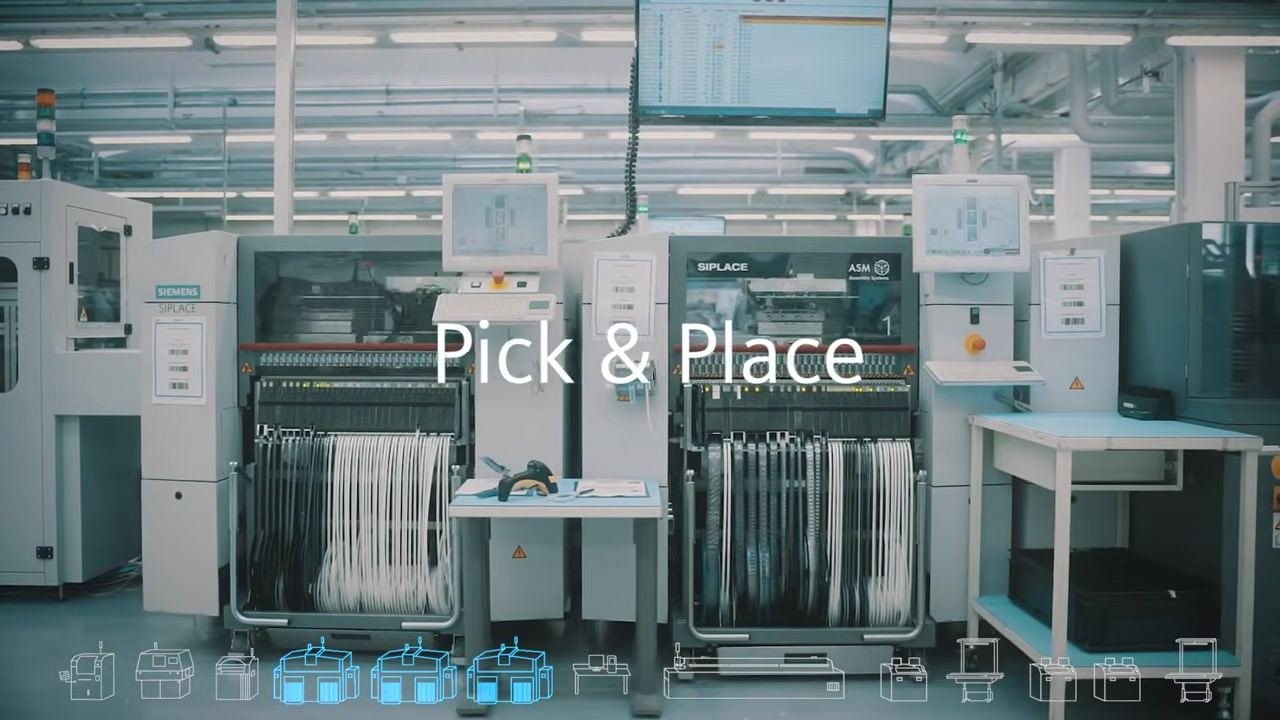
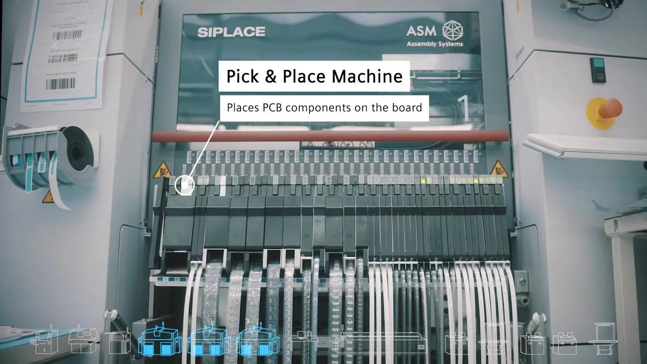
Step 11 — Identify the applicable pick and place machine. The facility uses three types of pick and place machines: a high-speed machine for rapid placement, a camera-guided machine for precise placement of small components, and a high-force machine for components requiring significant insertion pressure (e.g., SIEMENS SIPLACE, ASM Assembly Systems).
Step 12 — Place components onto the board. The pick and place machine automatically places components onto the PCB according to the assembly program, using multiple feeders and, where applicable, vision systems for accuracy.
Step 13 — Apply high-force placement where required. For boards requiring additional insertion force, use the specialized high-force pick and place machine.
Step 14 — Generate the assembly program. Use Valor Process Preparation software to create the program controlling the pick and place machines, ensuring each job is configured for the specific product and revision.
Step 15 — Manage component materials. Use Valor Material Management to track material usage and prompt replacement when materials are consumed. Valor IoT connects to the machines to collect utilization data, and Opcenter Execution Electronics may be integrated for execution management. Operators load or replace component reels at the feeders as needed.
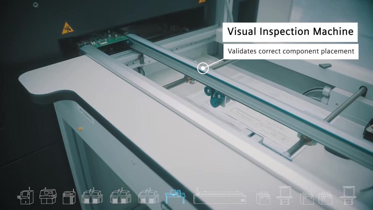
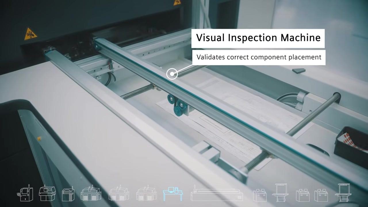
Step 16 — Perform visual inspection. At the visual inspection station, confirm that the correct components have been placed on the board before proceeding to the next stage.
Step 17 — Validate placement using generated documentation. Use the inspection documentation created by Valor Process Preparation to confirm correct component placement.
Phase 5: Soldering, oven profiling, and post-SMT inspection
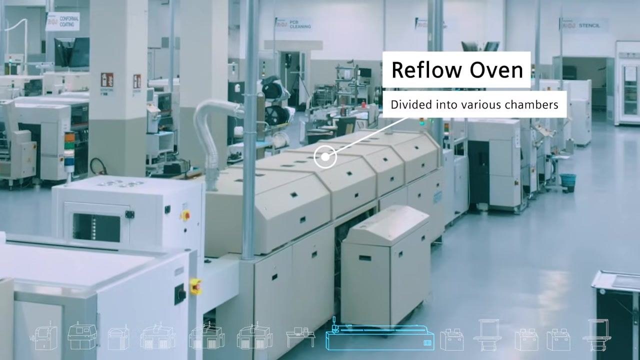
Step 18 — Pass the PCB through the reflow oven. The reflow oven is divided into several chambers, each capable of operating at different speeds and temperatures. Valor IoT Manufacturing connects to the oven to receive real-time data on actual temperature and conveyor speed for each chamber.
Step 19 — Monitor and adjust oven parameters. Confirm each chamber is set to the required temperature profile for the PCB assembly, and adjust conveyor speed as needed to meet soldering requirements.
Step 20 — Inspect the PCB after reflow soldering. At the inspection station, verify correct component placement, correct angle, and solder joint quality using automated equipment that examines pin-to-pad contact points.
Step 21 — Perform Automated Optical Inspection (AOI). Use the AOI machine (e.g., Omron VT-RNS) to automatically scan the PCB for placement accuracy and soldering quality. Review results on the labeled "Automated Optical Inspection (AOI)" monitor.
Step 22 — Validate results with Valor Process Preparation. Use test programs generated by Valor Process Preparation to specify inspection locations and validate placement and soldering of all components.
Step 23 — Perform through-hole and manual assembly. For components not suitable for SMT, manually insert components at the through-hole station, then solder them automatically using the selective soldering oven (e.g., ERSA VERSAFLOW 3/45).
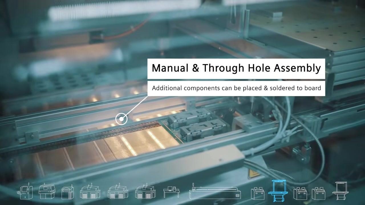
Step 24 — Solder additional manually placed components. Place and solder any additional components required using the selective soldering process.
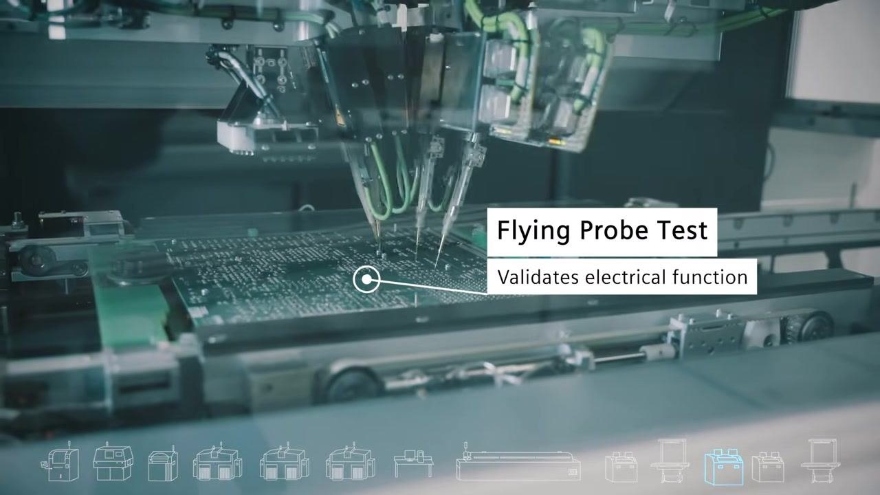
Step 25 — Perform electrical testing. Two methods are available: - Bed of Nails — suited to high-volume production; enables rapid testing but requires custom fixture development. - Flying Probe — suited to high-mix, small-volume production; takes longer to program and test but offers flexibility for new products.
Electrical testing stations are labeled (e.g., SPEA 3030 Board Tester).
Step 26 — Run the Flying Probe test. The flying probe tester automatically moves probes to contact PCB test points to validate electrical function. Valor Process Preparation can generate the corresponding test program.
Step 27 — Collect and manage test data. Valor IoT collects data from all testers, including electrical measurements and pass/fail results, for use in traceability, quality control, and process improvement.
Phase 6: Final integration, inspection, and delivery
Step 28 — Confirm system integration. Ensure all Valor manufacturing solutions are fully integrated within the CamStar Electronic Suite to enable seamless data flow and process management across the manufacturing floor. No manual action is required at this system-level integration step.
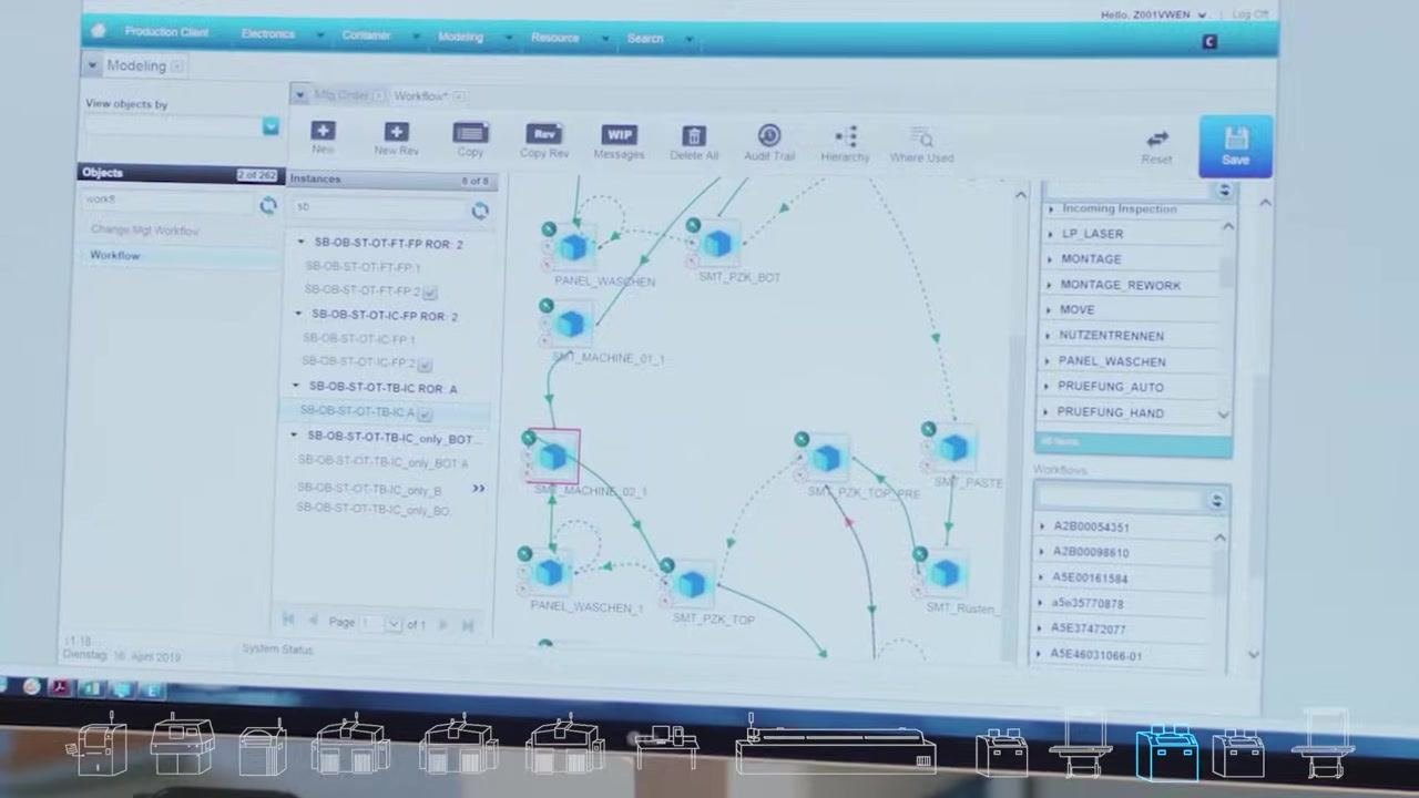
Step 29 — Verify BGA component pin connectivity. For large Ball Grid Array (BGA) components, use the CamStar suite's modeling and workflow tools to trace and verify that pins reach the correct PCB layer. Navigate to the workflow diagram and inspect connectivity paths.
Step 30 — Perform X-ray inspection. Use the X-ray inspection system to capture an X-ray image of the PCB and confirm adequate soldering and connectivity of BGA and other components. Operate the machine via the control panel and review the resulting images on the monitor.
Safety note: Follow posted X-ray warning signs and safety procedures at this station.
Step 31 — Perform functional testing. After inspection, initiate functional testing of the assembled product using the control panel (joysticks, buttons, keyboard). Confirm all test parameters are set according to product requirements.
Step 32 — Prioritize early defect detection. Resolve defects during earlier inspection and process steps rather than waiting for final functional test. Use in-process inspection equipment and test fixtures to identify issues as early as possible.
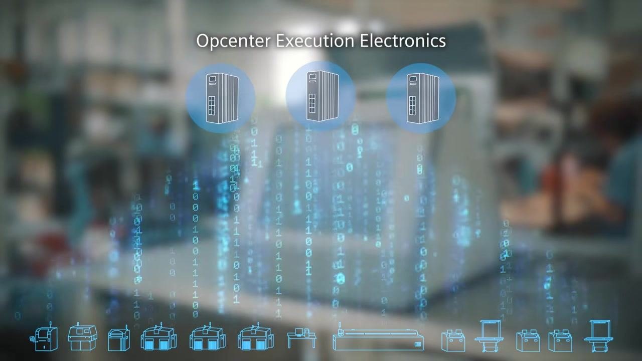
Step 33 — Prepare the product for delivery. Once all tests pass and quality standards are met, mark the product as ready for delivery. The system may display a completion screen, such as "Opcenter Execution Electronics," confirming the process is finished. No further manual action is required.
Verification and Summary
Step 34 — Confirm end-to-end process completion. Review the exterior of the "ROJ" manufacturing facility to confirm that the full process, from PCB serialization through final testing, has been completed at a professional, integrated production site.
Step 35 — Acknowledge the technology provider. The integrated manufacturing solutions used throughout this process are provided by Siemens, under the slogan "Ingenuity for life."
By completing these steps, Valor Manufacturing Solutions are fully integrated, inspected, tested, and delivered through the CamStar Electronic Suite and Siemens Opcenter Execution Electronics, ensuring the highest standards of quality and efficiency in PCB manufacturing.
Generation details: cost, quality tiers
Docsie billed 3,500 credits ($2.45) to analyze this 7-minute video at standard quality. The rewrite, template fill and Word/PDF exports were included. The same video at each quality tier:
| Quality | Frames sampled | Credits | Approx. cost |
|---|---|---|---|
| Draft | every 16-30 s | 1,750 | $1.22 |
| Standard (this guide) | every 8-15 s | 3,500 | $2.45 |
| Detailed | every 4-7 s | 7,000 | $4.90 |
| Ultra | every 1-3 s | 14,000 | $9.80 |
Credits priced at $0.70 per 1,000; plans include a monthly allowance. Enterprise customers on on-premise or bring-your-own-model deployments run this on their own inference and pay no per-video credits.
Generated by Docsie Video-to-Docs on 2026-09-08 from a 6-minute video. Screenshots are frames from the source video and belong to their creator, Siemens Software, whose original is embedded above. If you own this video and want the guide removed or credited differently, contact us and we will act within one business day.